We use LTspice, an open source analog circuit simulator to simulate systems of coupled DPLL on the level of the voltage and current time-series.
Using this industry-standard approach to test the circuit architectures down to the transistor level before setting up the prototype systems for experimentation allows to identify potential problems such as parasitic resistances and capacitances. We also use it to gain a better intuition on the dynamics within the circuitry as components become heterogeneous and are subject to noise.
Here we present our current ongoing work on a system of mutually delay-coupled digital phase-locked loops (DPLLs), each consisting of a phase detector (here XOR), a loop filter (first order RC-filter low pass) and a voltage-controlled oscillator (VCO), specifically the LTC6900 model from Analog Devices.
We couple these DPLLs with each other and without a time reference and consider signal transmission, feedback and processing delays in the network and the nodes. The concept behind this setup is a publications in PLOS ONE and the New Journal of Physics, titled Self-organized synchronization of digital phase-locked loops with delayed coupling in theory and experiment and Synchronization in networks of mutually delay-coupled phase-locked loops. In these publications the frequencies and phase configurations of self-organized synchronized states and their stability are analyzed for networks of analog and digital phase-locked loops using a phase model. In such networks different types of synchronized states exist, for which the frequencies of all PLLs can adjust to a common global frequency in a non-linear dependence on the time-delays and the coupling strengths, while different phase configurations are possible. These states with the different phase configurations are called splay or m-twist synchronized states. Whether such states are stable strongly depends on the transmission-delay between the oscillators, the coupling strength and the internal process of the oscillator nodes, such as signal filtering and feedback delay-times.
We start with a system of  mutually delay-coupled DPLL clocks running at a mean intrinsic frequency of
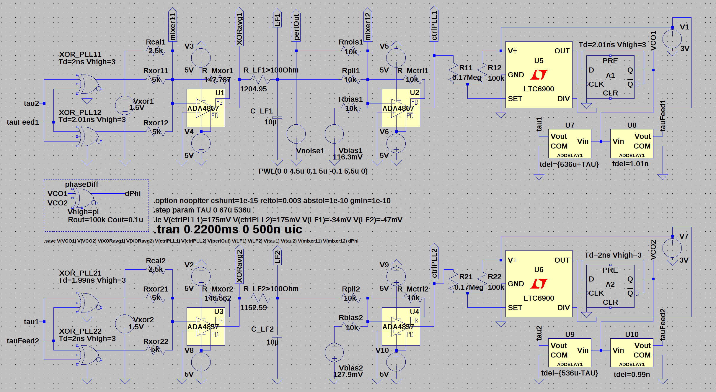
  MHz, see Fig. 1: LTspice block level circuit diagram of two delay-coupled DPLLs. Before that, we perform a separate SPICE simulation to measure the input response of the voltage-controlled oscillator, in this case a LTC6900, of our DPLLs. Hence we perform a parameter sweep transient simulations for each of which we change the input voltage to the LTC6900 VCO and measure the frequency of the output signal. We obtain the frequency from a Fourier analysis, using the FFT tool of the LTspice software. The result is shown in Fig. 2: VCO response curve. Note that we use a d-flip-flop at the output of the LTC6900 that divides the frequency by a factor two and ensures a duty cycle of 50%.
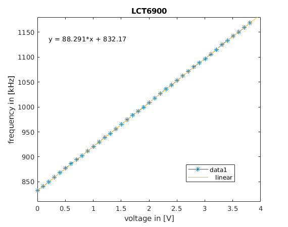
The slope of the linear fit is the input sensitivity of the VCO with  MHz/V and the free running frequency
  MHz. As can be seen from the circuit diagram, the output signals of the two (here redundant) XOR phase detectors are mixed together with a shift voltage
  . The mixer is designed such that it takes into account all XOR outputs, that potentially originate from different coupling pairs, equally. makes the center frequency of the full setup adjustable and sets the operation point. This part is followed by the loop filter, here a first order RC low pass, whose output is fed into a second mixer that combines the offset signal
  . The offset signal can also shift the center frequency of the VCO, as will become clearer in the following. In the next step, we establish how the parameters of the SPICE circuit level simulations translate to the parameters of the phase model. With this we bridge the gap between these two abstraction layers. The phase model reads
(1) ![\begin{equation*} \dot{\phi}_k(t)=\omega_k+\frac{K_k}{n_k}\sum\limits_{l=1}^N\,\text{d}_{kl}\int\limits_0^{\infty}\text{d}u\,p_k(u)\,h\left[\phi_l(t-u-\tau_{kl})-\phi_k(t-u-\tau_{kl}^f) \right] \end{equation*}](https://lucas-wetzel.de/wp-content/ql-cache/quicklatex.com-561b237658c4465000232800361f5bb6_l3.png "Rendered by QuickLaTeX.com")
where  indexes the PLLs in the network,
  denotes the instantaneous frequency,
  the intrinsic frequency,
  the coupling strength,
  the number of input signals to PLL ,
  the impulse response of the loop filter,
  the transmission-delay of a transmission delay line between nodes and
  ,
,  the feedback delay-time in the feedback path within PLL to the input of PLL , and the
  are either one or zero, depending on whether there is a connection or not. The parameters of the phase model have the following connection to the parameters of the LTspice circuit simulation
(2) 
where denotes the intrinsic frequency in the phase model and the coupling strength,  of the XOR output, and
  the scaling factor that scales the input sensitivity
  . In the circuitry this scaling is implemented by a closed-loop operational amplifier (here inverting) that measures voltage differences at its (high impedance) input and outputs the this voltage amplified with an amplification factor given by the relation of the resistors
  and
and  .
.